How a two-die architecture shift signals the end of monolithic computing—and arrives at the worst possible moment for everyone else
Executive Summary
- Apple's March 3 launch of M5 Pro and M5 Max chips marks the company's first-ever chiplet design—its "Fusion Architecture" combines two separate 3nm dies into a single system-on-chip, validating an approach AMD pioneered seven years ago and sending shockwaves through the semiconductor industry.
- The announcement lands during a perfect storm: Samsung and SK Hynix shed $170 billion in a single session as the KOSPI crashes 7.2%, DRAM prices have surged over 100% in 12 months squeezing PC margins, and Samsung's own foundry struggles at its Taylor, Texas fab threaten to leave TSMC as the world's only viable advanced chipmaker.
- With Apple simultaneously launching the $599 iPhone 17e to attack the mid-market and committing $600 billion to US manufacturing, Cupertino is executing a three-front assault—architectural innovation, market expansion, and geographic diversification—that will force every major chip designer to respond within 18 months or risk permanent marginalization.
Chapter 1: The Architecture That Changes Everything
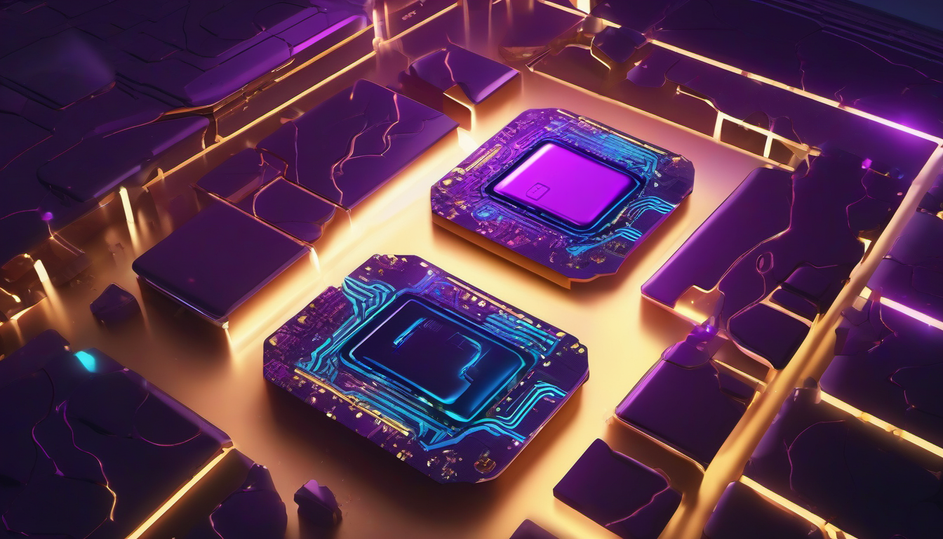
On March 3, 2026, Apple quietly rewrote the rules of chip design. The new M5 Pro and M5 Max processors powering the updated MacBook Pro lineup don't just deliver the expected generational improvements in speed and efficiency. They represent something far more fundamental: Apple's first departure from monolithic chip design.
Since the debut of the M1 chip in late 2020, Apple Silicon has been built on a single-die philosophy. Each chip—from the base M1 through the M4 Ultra—was essentially one continuous piece of silicon carved from a TSMC wafer. The Pro variants doubled resources by scaling the design; the Max variants quadrupled them. But they remained monolithic: one die, one package.
The M5 Pro and M5 Max break this pattern entirely. Apple's new "Fusion Architecture" physically combines two separate third-generation 3-nanometer dies into a unified system-on-chip using TSMC's advanced packaging technology. The two dies communicate through high-bandwidth, low-latency interconnects, presenting themselves to software as a single coherent processor. The result: an 18-core CPU with six "super cores" (Apple's new designation for its highest-performance cores) and 12 efficiency-optimized performance cores, paired with up to 40 GPU cores, each embedded with a dedicated Neural Accelerator for AI workloads.
The numbers tell a story of radical improvement. AI performance leaps 4x over the M4 generation. LLM prompt processing is 3.9x faster. GPU ray tracing improves 35%. But the real revolution isn't in the benchmarks—it's in the manufacturing economics.
A monolithic chip is limited by the maximum practical die size a foundry can produce. As dies grow larger, manufacturing yields drop exponentially—a single defect anywhere on a 600mm² die renders the entire chip useless. By splitting the design into two smaller dies and connecting them through advanced packaging, Apple can achieve the performance of a massive monolithic chip while manufacturing each half at significantly higher yields. This is the same insight that propelled AMD from near-bankruptcy to competitive parity with Intel beginning in 2019, when it introduced its Zen 2 processors using a chiplet architecture.
Apple's adoption of this approach is the definitive validation. When the world's most valuable company—with the resources to push monolithic design to its absolute limits—chooses chiplets instead, the message is unmistakable: the monolithic era is over.
Chapter 2: The Perfect Storm in Memory and Manufacturing
Apple's architectural pivot arrives during one of the most stressful periods in semiconductor history. The same week Apple launched its new Macs, South Korea's stock market suffered its worst single-day crash in 19 months.
On March 3, the KOSPI plunged 7.24% to 5,791.91 as markets reopened after a holiday to face the reality of Operation Epic Fury and the Hormuz Strait crisis. Samsung Electronics fell 10%, SK Hynix dropped 11.5%, and the two companies lost a combined $170 billion in market capitalization in a single session. Foreign investors dumped over $3 billion in Korean equities.
But the KOSPI crash, while dramatic, obscures a more structural vulnerability. DRAM prices have surged over 100% in 12 months as chipmakers redirect manufacturing capacity toward high-bandwidth memory (HBM) for AI accelerators, starving the consumer electronics market. NAND flash prices have climbed 87%. These are critical components in every laptop, smartphone, and tablet sold worldwide.
Apple acknowledged this reality implicitly. The new MacBook Air starts at $1,099 with 512GB storage—effectively a price reduction, since the previous generation charged $1,199 for the same storage tier. The MacBook Pro starts at $2,199 with 1TB standard. Apple is absorbing memory cost increases to maintain price points, a luxury its competitors cannot afford. With over $160 billion in annual free cash flow and $65 billion in net cash, Apple can subsidize hardware margins in ways that Dell, HP, Lenovo, and Acer simply cannot match.
Meanwhile, Samsung's foundry ambitions continue to falter. The company's Taylor, Texas fabrication plant—a cornerstone of US semiconductor reshoring—has pushed back mass production of 2nm chips to 2027, widening the gap with TSMC. Samsung's Gate-All-Around (GAA) transistor yields remain problematic, and major customers like Tesla are reportedly reconsidering their commitments. Apple's Fusion Architecture, built on TSMC's proven 3nm process and advanced packaging, underscores just how dependent the industry has become on a single Taiwanese manufacturer.
| Metric | Apple (TSMC) | Samsung Foundry | Intel Foundry |
|---|---|---|---|
| Advanced node (3nm) | Mass production since 2023 | Limited yield, delayed | 18A expected late 2026 |
| Chiplet packaging | Fusion Architecture (SoIC-class) | Limited offerings | EMIB/Foveros (niche) |
| Major customers | Apple, AMD, Nvidia, Qualcomm | Tesla (wavering), Google | Internal + limited |
| 2026 capex | ~$36B (TSMC total) | ~$8B (foundry portion) | ~$25B (with CHIPS subsidies) |
| Yield at leading edge | >80% estimated | <50% estimated | Unknown |
Chapter 3: The Three-Front War
Apple's March 2026 "Big Week" isn't just a product refresh. It's a coordinated strategic offensive across three dimensions simultaneously.
Front 1: Architectural supremacy. The Fusion Architecture doesn't just improve Apple's own products. It signals to every chip designer—Qualcomm, MediaTek, Nvidia's nascent ARM PC efforts—that Apple is now playing the same architectural game as AMD, but with TSMC's most advanced packaging technologies and Apple's unmatched design resources. Qualcomm's Snapdragon X Elite, which finally brought competitive ARM performance to Windows PCs in 2024, remains a monolithic design. It will need to match Apple's chiplet approach or face permanent disadvantage in performance-per-watt scaling.
Front 2: Market expansion. The iPhone 17e at $599 represents Apple's most aggressive mid-market play in years. Starting at 256GB with Apple's latest chip, it targets the vast population of Android users who have never considered an iPhone, as well as the hundreds of millions of aging iPhone SE and iPhone 12/13 owners. Similarly, Apple is rumored to announce a budget MacBook later this week—possibly running on an iPhone-derived chip—that could attack the Chromebook market directly. If Apple can offer a $799 MacBook, it fundamentally changes the competitive landscape in education and enterprise entry-level computing.
Front 3: Geographic diversification. Apple's $600 billion US manufacturing commitment, announced weeks earlier, includes TSMC's Arizona fabs producing over 100 million chips annually, Amkor's $7 billion packaging facility, and GlobalWafers' $4 billion silicon wafer plant. The Fusion Architecture's reliance on advanced packaging means these US facilities aren't just assembling products—they're performing the most technologically demanding steps in chip production. This positions Apple uniquely among tech giants: it can claim genuine US manufacturing while leveraging the world's most advanced semiconductor technology.
Chapter 4: The TSMC Question
Apple's Fusion Architecture depends entirely on TSMC's advanced packaging capabilities—likely a variant of the company's System-on-Integrated-Chips (SoIC) technology combined with its Integrated Fan-Out (InFO) platform. This deepens Apple's already extraordinary reliance on a single foundry.
TSMC fabricates every Apple-designed chip: every iPhone, iPad, Mac, Apple Watch, and Vision Pro processor. It now also provides the advanced packaging that makes Apple's chiplet architecture possible. No other foundry on Earth can replicate this combination of leading-edge node manufacturing and heterogeneous die integration at scale.
This concentration creates a paradox. Apple's Fusion Architecture is a triumph of design innovation, but it also tightens the chokepoint. If TSMC's operations were disrupted—by natural disaster, geopolitical conflict, or capacity constraints—Apple would have no fallback. Samsung's foundry cannot match TSMC's yields; Intel Foundry Services remains years away from competitiveness at the leading edge.
The geopolitical implications are stark. TSMC's most advanced fabs remain in Taiwan, specifically in Hsinchu and Tainan. While the Arizona fabs are producing chips on older nodes (initially 4nm, with 3nm planned), the most advanced packaging technologies that enable Fusion Architecture are concentrated in Taiwan. Apple's chiplet revolution, paradoxically, makes the Taiwan Strait an even more critical chokepoint for global technology supply chains.
This is why Apple's $600 billion US investment matters beyond public relations. If TSMC can replicate its advanced packaging capabilities in Arizona—and if Apple's Amkor partnership can provide an alternative packaging pathway—Cupertino begins to build redundancy into a supply chain that currently has none. But this transition will take years. In the interim, every M5 Pro and M5 Max chip will be manufactured and packaged in Taiwan.
Chapter 5: Scenario Analysis
Scenario A: Chiplet Dominance Accelerates (45%)
Thesis: Apple's validation of chiplet design triggers an industry-wide shift within 18 months. Qualcomm, MediaTek, and even Nvidia's ARM PC division adopt multi-die architectures for their next-generation products.
Evidence:
- AMD's chiplet strategy, introduced in 2019, enabled it to surpass Intel in server market share by 2025—proving the approach works at scale.
- TSMC reported advanced packaging revenue grew 60%+ in 2025, with demand outstripping supply.
- Intel's own tile-based architecture (Meteor Lake, Arrow Lake) already uses heterogeneous die integration, though with less commercial success.
Trigger conditions: Qualcomm announces a multi-die Snapdragon for 2027; TSMC expands CoWoS/SoIC capacity by 50%+ in 2026-2027.
Investment implications: TSMC and advanced packaging equipment makers (BESI, ASM Pacific) benefit most. Apple solidifies its ecosystem premium. Intel faces existential pressure as its foundry offering cannot match TSMC's packaging.
Scenario B: Memory Bottleneck Constrains Adoption (35%)
Thesis: Surging memory prices and supply constraints limit the market impact of Apple's new products. PC industry margins compress further, delaying the broader chiplet transition.
Evidence:
- DRAM prices up 111%, NAND up 87% in 12 months, driven by AI-driven HBM reallocation.
- The broader PC market faces uneven demand; consumers and businesses delay upgrades.
- The KOSPI crash and $170B Samsung/SK Hynix wipeout reflect market anxiety about semiconductor demand sustainability.
Trigger conditions: DRAM prices rise another 30%+ by Q3 2026; PC shipments decline year-over-year; Apple's Mac revenue misses expectations for two consecutive quarters.
Investment implications: Memory makers face volatile swings. Apple's massive cash reserves provide a buffer, but smaller OEMs (HP, Dell, Acer) face margin pressure. Budget MacBook launch could be delayed or priced higher than expected.
Scenario C: Samsung Foundry Collapse Reshapes Industry (20%)
Thesis: Samsung's continued foundry struggles lead to major customer defections, effectively creating a TSMC monopoly in advanced chip manufacturing. This triggers regulatory concern and accelerated reshoring efforts.
Evidence:
- Samsung Taylor, Texas fab delayed to 2027 for 2nm mass production.
- Tesla, Google, and other customers reportedly reconsidering Samsung foundry commitments.
- Samsung's foundry division posted operating losses in 2025.
- Apple's Fusion Architecture demonstrates what's possible only with TSMC—widening the perception gap.
Trigger conditions: Tesla formally shifts AI chip production to TSMC; Samsung announces foundry restructuring; US CHIPS Act officials redirect subsidies toward TSMC expansion.
Investment implications: TSMC's pricing power increases substantially. Samsung's semiconductor division faces a reckoning between memory (strong) and foundry (weak). Intel Foundry Services becomes the only plausible Western alternative, potentially attracting government subsidies despite technical gaps.
Chapter 6: Investment Implications
Direct beneficiaries:
- TSMC (TSM): Apple's deepening reliance on advanced packaging cements TSMC's position. Revenue from advanced packaging alone could reach $15-20B annually by 2027.
- BESI, ASM Pacific, Kulicke & Soffa: Advanced packaging equipment demand surges as the industry follows Apple's chiplet playbook.
- Apple (AAPL): The Fusion Architecture creates a sustainable performance advantage that competitors need 18-24 months to match. The $599 iPhone 17e expands the addressable market by an estimated 200-300 million potential upgraders.
Under pressure:
- Intel (INTC): Apple's success with TSMC-based chiplets further undermines the case for Intel Foundry Services. Intel's own tile-based designs have not achieved comparable commercial success.
- Samsung Electronics (005930.KS): The combination of foundry struggles, war-driven market crash ($170B wipeout), and Apple's TSMC-exclusive chiplet strategy compounds Samsung's competitive challenges.
- Windows PC OEMs: Rising memory costs squeeze margins; Apple's ability to absorb these costs through vertical integration and scale creates an unfair advantage. Dell, HP, and Lenovo face a tightening vise.
Watch list:
- Qualcomm (QCOM): Must respond to Fusion Architecture with its own multi-die design or risk losing ground in the premium laptop market it only recently entered.
- AMD (AMD): The original chiplet pioneer benefits from industry validation but faces Apple as a direct competitor in high-performance ARM computing.
- Amkor Technology (AMKR): Apple's $7B partnership positions Amkor as a critical packaging alternative to TSMC's in-house capabilities.
Conclusion
Apple's Fusion Architecture is more than a chip upgrade. It's a declaration that the semiconductor industry's center of gravity has permanently shifted from raw transistor shrinks to system-level integration through advanced packaging. When Apple—a company that could afford to push monolithic design further than anyone else—chooses chiplets instead, every other chip designer receives the same message: adapt or fall behind.
The timing is both strategic and fortunate. As geopolitical turmoil crashes semiconductor stocks, as memory costs squeeze margins across the industry, and as Samsung's foundry struggles leave TSMC without a peer, Apple's architectural leap cements its position at the apex of the technology supply chain. The company that once nearly went bankrupt now dictates the trajectory of a $600 billion industry.
The question isn't whether the chiplet revolution will transform computing. Apple just answered that. The question is who else can execute it—and who gets left behind.
Sources: Apple Newsroom, 9to5Mac, CNA, Fortune India, Bloomberg, Seoul Economic Daily, MacRumors, TradingKey
Leave a Reply